|
Believe
it or not, there was a day when building your own electronics was
a good way to save money if your budget was smaller than your appetite
for R/C systems, radios, even TV sets. Heathkit comes to mind for
all us old-timers as a source of pre-kitted products, but like most
electronics companies of yore, they no longer offer kits; it is
much cheaper to have complete systems built overseas. Besides, modern
components - resistors, capacitors, ICs, etc., are far too small
for most people to work with successfully. Here is a two-part article
from the April and May 1972 editions of American Aircraft Modeler
showing how it was done with a custom 2-channel digital proportional
radio control system dubbed the AAM Commander. It still makes a
good read because of the theory of operation that is covered.
AAM Commander
Part II (see
Part I, April 1972 AAM)
High-speed switching of integrated circuits requires special
design features used in the high-power IC transmitter and three-wire
IC servo presented this month. By Fred Marks
In the preceding issue, we described the entire system, presented
the printed circuit layout and the parts list, with in-formation
useful in procuring parts, and illustrated some preliminary assemblies
to be made in advance for building the transmitter. This issue will
contain instructions for transmitter and servo assembly plus the
design information for them. Since it may be confusing to pull the
design information for individual units from context, we shall review
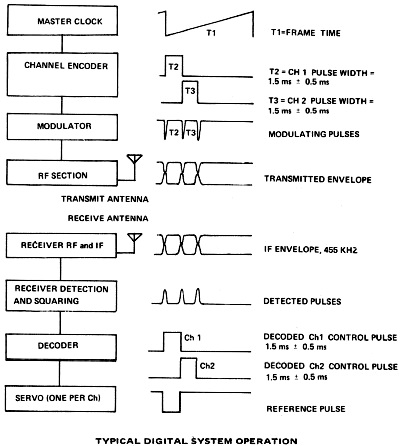
the operation of digital systems. Overall functioning of
the system is shown in a simplified form by the block diagram and
approximate waveforms in Figure 1. More detailed block diagrams
and schematics for the sub-functions will be presented in the discussion
of individual units. The frame time (T1) is set by the master
clock, in this case a relaxation oscillator, at about 14 milliseconds.
The inverse, or frame rate, is 1000 divided by 14 or about 70 frames
per second. In other words, the servos will receive new command
information 70 times each second.
Tuning the AAM Commander 2-Channel R/C System
System Waveforms
Transmitter PCB Component Layout
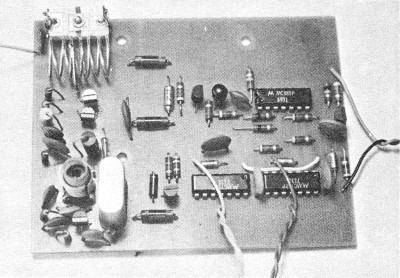
Transmitter PCB Assembly
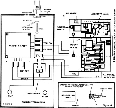
Transmitter Wiring Diagram
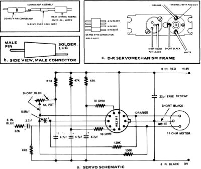 Servo
Schematic & Wiring Diagram Servo
Schematic & Wiring Diagram
Servo Component Assembly
Servo Component Layout
Servo Wiring
The sharp fall at the end of the sawtooth ramp is differentiated
to produce a synchronization pulse that is transmitted, but also
starts the channel encoder to work by initiating the pulse, identified
by time period T2. T2 is variable by the Channel 1 control pot from
a nominal 1.5 ms to as short as 1.0 ms or as long as 2.0 ms. The
sharp fall of the trailing edge of the Channel pulse is also differentiated
and transmitted but simultaneously initiates the Channel 2 control
pulse. The Channel 2 pulse length is variable just as the Channel
1 pulse. The trailing edge of the Channel 2 pulse is also differentiated
to form a spike and is transmitted. The actual transmitted
envelope is a continuous wave at the desired R F frequency with
three short modulation pulses separated by T1 and T2. The receiver
accepts the R F envelope and detects, or reconstructs, the original
modulating pulses. The decoder acts upon these three pulses to reconstruct
the original control pulses (T1 and T2) and route them to the servos
for the respective channels. The servo accepts the decoded
pulse of duration T1 routed to it and compares the length of that
pulse to a reference pulse whose length is set by a feedback potentiometer
in the servo. At neutral the length of the reference pulse is 1.5
ms. The objective is for duration of the servo reference pulse to
exactly match the duration of the control pulse. When they differ,
the servo output moves in the appropriate direction to nullify the
error. Since new information is being received by the servo 70 times
per second, motion is smooth and precise, which was the objective
of the whole process. The transmitter, receiver, and decoder can
be simulated by a simple servo tester as far as the servo is concerned.
Transmitter Design The transmitter
was designed for ease of building and adjustment. Output power is
relatively high-approximately one watt into the final stage when
operated at 9.6 volts. The oscillator is stable and broad with primary
frequency control provided by the crystal. Refer to Figure
2a, the block diagram, and Figure 2b, the schematic, for the following
discussion. The transmitter is designed exactly like the block diagram
and will be discussed in the order from bottom to top. The schematic
is laid out exactly the same, and (surprise!) so is the transmitter
P.C. board. The master clock is oblivious to anything else
going on in the transmitter - it simply generates a 6V amplitude
sawtooth every 14 milliseconds. This master clock consists of Q1,
C1, R1, R2 and R3. The repetition rate may be changed by varying
the value of R3. The falling edge of the sawtooth is differentiated
by R4 and C2 to form the synchronization pulse (a 1.5V amplitude
spike), which is the first in the series of the three required for
a two-channel system. This pulse also serves as the clock pulse
for the first control pulse generator which is a monostable or one
shot, multivibrator M1, formed of the gates of IC1 (see schematic).
It also connects to the input of Expander E1. The first
one shot is used for Channel 1 in this system and is formed of G1,
G2, C3, and the rudder control pot. When G1 is "clocked" by the
synchronization pulse, it flips to the "on" condition at its output
until C3 completes its discharge through G1, G2, and the control
pot. The position of the control pot determines the length of time
that M1 remains "on"-nominally 1.5 milliseconds and ± 0.5 milliseconds.
The trailing edge of this 3.6V square Wiring in the ACE case with
the Rand stick assembly is short and direct. P.C. board has been
moved aside for clarity. pulse is differentiated by R5 and
C4. This differentiated pulse (a spike 1.5V in amplitude) "clocks"
the second one shot multi (M2) and also is fed to the second input
of Expander E1. The second control pulse generator for Channel
2 is formed by G5 and G6 located in IC2. It functions precisely
the same as M1, except that it is controlled by the Ch. 2 control
pot. The trailing edge of the 1.5 ms square pulse for Ch. 2 is differentiated
by R6 and C8 and is fed to one input of Expander E2. The
three spikes generated as just described (i.e., the differentiated
output of the master clock pulse, first control pulse generator,
and second control pulse generator) are fed to the quad expander
(IC3). The expander functions in the same manner as a gate but introduces
some gain, is capable of handling greater output loading, and widens
the spikes slightly by some integration performed by R7 and C7.
The output of the expander is the train of three pulses with amplitude
of 3.5 volts and a width of nominally 250 microseconds. The
chore of modulation is too much for inexpensive ICs, so the output
from the pulse expander is amplified and shaped by the modulator
formed by CB, Q2, R11, R1O and R12. The ICs require 3.B
volts; rather than using a tapped battery supply, a regulator is
used to derive 3.B volts from the 9V transmitter supply. This is
a simple device consisting of ZI (a reference Zener diode) which
senses output and controls the bias on Q4 which has a high impedance.
Thus little current is wasted. L1, L2 and L3 simply isolate
the RF section from the encoder/modulator. The R F oscillator consists
of Q5, the crystal, C11, R15, R17, C12, C13 and L4. The inductive/capacitive
(LC) circuit L4/C13 and the crystal set the frequency. The resistive/capacitive
(RC) circuits shown (R17/C12 and RI5/C11) reduce the possibility
of undesired harmonics. The output is a sine wave at the desired
frequency approximately 0.2 volts in amplitude. The output
of the oscillator is coupled to L5 and is amplified by the output
transistor, Q6. Modulation is introduced via the 47 mF capacitor
(C10) coupling to the modulator Q3 via L2. This capacitor, in effect,
shows the base of Q6 a direct short to ground each time a pulse
is received from the encoder/ modulator, however the rise and fall
of the modulating pulse is carefully shaped by C10, C14, R18 and
the modulator to avoid unwanted harmonics. The RF amplifier
takes the input from the oscillator and increases the amplitude.
Since transistors can also amplify unwanted harmonics, a final trap
formed by inductor L7 and C 17 is used to tune the output stage
and match the impedance of the output transistors. The output is
coupled capacitively to the antenna by C19. There are a
few points of interest regarding the output section. The output
transistors are paralleled for somewhat greater output but at the
expense of current drain. The use of the heat sink provides a margin
for the transistor and we have operated the transmitter on from
9 to 12 volts. Operation becomes unsatisfactory when battery voltage
goes below about 7.5. No metering circuit is provided for the sake
of simplicity. If the planned use for the system is a boat or car
installation, Q7 and R20 may be deleted to reduce output and, thus,
current drain. However, the use of the heat sink on Q6 then becomes
a necessity. Servo Design The servo
is based on application of the World Engines integrated circuit,
manufactured for them by Signetics, Inc. Figure 3a presents the
schematic for the servo amplifier. Our overall amplifier design
is essentially the same as that used by World Engines. One resistor
was Changed to obtain the proper damping margin with the rather
quick, small D-R servos. A new, tighter P.C. layout was used to
permit installation in the smallest servos . The use of
the World Engines IC introduced some unique problems, not in the
design of the servo but of the receiver. Filtering of receiver power
supply must be good because the IC amplifier switches so rapidly
that electrical spikes are generated in the power supply. I have
seen two other servo amp designs which use the same chip and each
has several changes, presumably in an attempt to overcome the electrical
spiking. We felt constrained to use enough filtering in the receiver
to permit the use of alkaline energizers, which are more susceptible
to electrical spiking because of their slightly higher internal
resistance (compared to nickel-cadmium cells). The problem is not
severe enough to require use of an active filter but any tighter
servo performance certainly will. The servo amplifier is
a bridge circuit-a two-wire battery pack can be used. It is the
equivalent to a discrete component bridge amplifier requiring 14
transistors and 34 discrete components. It actually has 31 transistors
on the chip. Basically the amplifier performs the same function
as any other, but most of the action is internal to the chip. The
design has one nicety that further helps reduce failure-only two
wires are required to the feedback pot meaning one less wire to
break. No arc suppression components need be mounted on the motor,
making it a clean installation. The servo will operate satisfactorily
from 3.6 volts. However, it will not tolerate the added drop of
a diode so that the use of a bypass diode on a failed battery will
not guard against battery failure. This servo does offer the potential
for use with a 3.6V system with slightly reduced power and speed.
Resolution of the amplifier with both D-R servomechanisms
is outstanding. Average thrust is about 2.75 lb. at a radius of
0.3 in. for an output torque of 0.92 in.-lb. Transit time is approximately
0.6 sec. Resolution was measured to be 0.25 degrees. The servo is
quite capable of measuring stick slop. Angular throw with the transmitter
is ± 40 degrees and trim is ± 8 degrees. Stability, resolution,
and transit time at 0°F and 150°F were found to be unchanged.
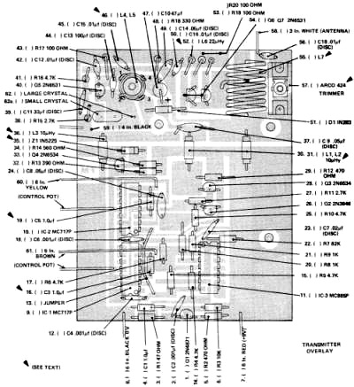
Assembly Instructions for Transmitter and Servos*
Check the components obtained against the components list
in the April issue. Study the overlay drawing (Figure 5), then drill
the hole beneath the enter of the ARCO 424 trimmer and beneath the
center of L4/L5 to 3/16-in. diameter. Drill the three unoccupied
holes marked by the bulls eyes to 1/8 in. to accept mounting screws.
Drill three holes for L7, two for C17, four for L3/L4, and (if a
large crystal is used) for the crystal pins; to 5/64 inch diameter.
Clean the P.C. board thoroughly with steel wool.
Proceed
to assemble all components on the pc board as shown on the overlay
drawings (Figure 5). Follow the numbered sequence as shown. The
basing arrangement for the transistors used was presented in the
last issue. Observe the identification of the IC's installed in
steps 9, 10 and 11. It would be embarrassing to have to desolder
14 pins if put in incorrectly. The 10 mH RF chokes L1, L2 and L3
installed in steps 30, 31 and 36 look like resistors with wire windings
on them. They require careful bending to fit in the holes. Observe
the polarity of the tantalum capacitors. Those made by Components
Inc. have the + end identified by a red cap. Sprague capacitors
have a + stamped on them. Do not confuse the identification of tolerance,
i.e., ± 20%, as the polarity identification. At step 35 where Z1
is installed, be sure to place the banded end as shown on the overlay.
Note that the crystal is installed at nearly the last step to protect
it. Provisions are made for either a small or a large crystal. At
step 46, L4 and L5 which were constructed earlier are installed
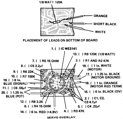
on the P.C. board. Looking at the overlay, terminals 1 and 2 are
to the left, 3 and 4 to the right (i.e., the hook-up wire secondary
goes to the right). RF chokes L1, L2 and L3 installed in
steps 30, 31 and 36 look like resistors with wire windings on them.
They require careful bending to fit in the holes. Observe the polarity
of the tantalum capacitors. Those made by Components Inc. have the
+ end identified by a red cap. Sprague capacitors have a + stamped
on them. Do not confuse the identification of tolerance, i.e., ±
20%, as the polarity identification. At step 35 where Z1 is installed,
be sure to place the banded end as shown on the overlay. Note that
the crystal is installed at nearly the last step to protect it.
Provisions are made for either a small or a large crystal. At step
46, L4 and L5 which were constructed earlier are installed on the
P.C. board. Looking at the overlay, terminals 1 and 2 are to the
left, 3 and 4 to the right (i.e., the hook-up wire secondary goes
to the right). At step 47, C10, a 47 uF tantalum is installed.
The positive polarity end as shown on the overlay is up-pointing
back toward the encoder. At step 51, be sure the banded end of the
diode is placed as shown. At step 52, L6, a 22tantalum is installed.
The positive polarity end as shown on the overlay is up-pointing
back toward the encoder. At step 51, be sure the banded end of the
diode is placed as shown. At step 52, L6, a 22 mH choke is installed.
This is a molded choke and looks quite similar to a resistor but
may be identified by the color code: silver, red, red, grey, silver.
At steps 54 and 55 install the output transistors Q6 and Q7.
The type shown is the Motorola 2N6531, however the GE 2N70BA may
be substituted in both the Q5, and Q6/Q7 locations. In step 57 position
the adjustment screw of C17 so that it reaches through the 3/16-in.
hole in the P.C. board. When P.C. board assembly is completed,
remove all solder resin with thinner and an old toothbrush. Check
the P.C. side of the board against Figure 6 to make certain there
are no solder bridges. The eight wires to be connected are shown
in Figure 6. Connecting the pots as shown (i.e., brown wires to
rudder pot) gives rudder on Channel 1 and elevator (yellow wires)
on Channel 2. Travel may be reversed by using the other end terminal
of the pot. After the wires are connected, check the resistance
between the 9V and 0 buss using a good quality ohmmeter. The resistance
should be about 150 ohms. If less, recheck for shorts or components
improperly installed. Cut three 9/16-in. lengths of the
outside section of Nyrod or fuel tubing for use as standoffs. Mount
the Rand stick assembly in the ACE case then mount the antenna fitting
and the switch. Mount the transmitter P.C. board to the Rand stick
using the three lengths of . tubing and 7/8-in. 4-40 screws. Check
to see that the screw heads do not touch the P.C. lands. If you
use any other stick assembly, you must provide an alternate method
of P.C. board attachment. Connect the ground lead of a voltmeter
to 0 volts. Check the supply voltage for 9V or more. Check the regulated
voltage at the emitter of Q4 - it should read close to 3.8 volts.
Connect the ground lead of an oscilloscope to 0 volts. Connect
the probe to the junction of capacitor C4 (see overlay) and pin
14 of IC1 with the stick and trim cent control pot so pulse is exactly
1.5 ms. Lock the control pot screw. Full stick movement should change
the pulse width by approximately ±0.5 ms. This sets rudder pulse
width. Repeat step 31 but with the probe placed at the junction
of capacitor C6 and pin 14 of IC2. This sets the elevator pulse
width. The RF section is tuned as follows but must be done
by a valid holder of an FCC second class license. One of three methods
may be used: (a) If a scope with sensitivity of 0.01 volts/cm
or less and a frequency range covering 27 MHz is available, simply
loop the probe lead twice around the extended antenna. Adjust the
slug in L4/L5 until a signal is seen and check to be sure the oscillator
recovers when the crystal is shorted by your thumb. Adjust the Arco
424 trimmer (C17) so that the amplitude of the displayed signal
peaks. (b) If a field strength meter is available, hold
the transmitter antenna nearby and adjust the slug in L4/L5 until
a reading is observed. Perform the same check of oscillator stability
as above. Adjust C17 for peak FSM meter reading. (c) If
a VTVM is available, construct a demodulator as shown in Figure
2c and use it and the VTVM as an FSM as in (b) above.
Servo Construction Check the fit of the
P.C. board in the servo case. When installing IC1, clip each of
the leads about 1/16 in. shorter than the preceding lead, proceeding
from one through eight. The shortest lead must be at least 1/4 in.
long. Leave the lead located at the tab full length. This permits
easier positioning and insertion of the leads. Install the
components in the order shown in Figure 7. Caution: Do not forget
the 1/8 watt, 120k resistor which goes on the bottom of the board.
Figure 10 is provided to show exactly where it goes. Cut the hook-up
wires to length, strip 1/8 in., tin, and solder in place on the
board. Note that the wires going to the motor are soldered to the
bottom of the board (Figure 7) not through holes drilled in the
board. Use dope thinner or alcohol and scrub all the resin from
the P.C. board. Prepare the feedback potentiometer element
as shown in Figure 11. Twist the six-in. blue, red and black leads
tightly and clip to the same length. Slip a rubber grommet over
the wires. Slip a 1/2 inch piece of 1/8 10 heat shrink tubing over
these three wires. Slip one of the pieces of sleeving provided with
the Deans four pin connectors over each wire. Strip 1/8 in. of the
ends of the three wires and tin. Tin three of the pins of the male
half of the Deans four pin connector (Figure 3b) and solder the
wires to their respective pins as shown in Figure 3b. Slip the sleeving
up over the pins and wires then re-twist them. Heat this tubing
with a soldering iron to shrink evenly, or use a lighted match.
Complete the wiring of the pot and motor as follows: Strip
1/8 in. from the ends of the short blue, white, black and orange
wires and tin. Prepare the potentiometer element by clipping the
lugs to one of the pot terminals and motor terminals as shown in
Figure 3c. The D-R Servomechanism is intended as a replacement
mechanism for a number of systems. Therefore, the small disc which
holds the pot wiper is not assembled. Mount the pot wiper as shown
in the D-R instructions and place the assembly on the wiper shaft
with the dual contacts which wipe the pot element centered toward
the motor end of the mechanism and with the output arm centered.
This can be checked by observing that the small stop pin on the
output gear is exactly in the center of the servo. Now, mount the
potentiometer element using the small screws provided with the mechanism;
position the pot element as shown in Figure 3c. This should automatically
place the pot wiper near the center of the element. This may be
checked with an ohmmeter; the resistances should be equalized between
the center and end below in white. too terminals of the pot. The
servo amplifier is sufficiently consistent that this gives a 1.5
ms servo reference pulse and may be used for setting up the system.
One then simply sets the transmitter control pots so that the servos
center. Do not place the motor in position yet. Plug in
the servo and turn on the transmitter and receiver. If interfacing
with a transmitter which has had pulse width set to 1.5 ms, slowly
rotate the servo output until the motor halts, reverses direction,
or pulses back and forth slightly. If the output is not centered
at this point, loosen the pot retention screws and rotate the element
slightly until the output is centered. Retighten the screws and
place the motor in position. The output should be centered and travel
should be smooth with a swing of about ±45 degrees. Place a 1/2
in. length of servo mount tape over the pot element to prevent shorts
to the solder lugs. Place a small square of foam padding against
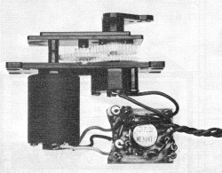
the servo amplifier bottom and assemble the servomechanism as shown
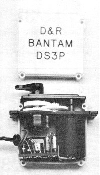
in its instructions. The servomechanism illustrated is manufactured
by D-R. The amplifier has been installed and tested in the Orbit
PS-4, Kraft KPS-12, and Controlaire S-4 servomechanisms. The amplifier
will undoubtedly work with almost any servo-mechanism made today.
However, it is relatively critical of decoder and receiver design
since it is designed to operate best with clean switching TTL integrated
circuit decoders. * These assembly instructions have
been edited heavily to permit their presentation in the limited
space available. Full instructions, in check-off format, are available
from ACE RIC upon request. The instructions provided here are adequate
to complete the assembly of the system, but must be followed carefully.
+The Editor.
|